
")
| Development of research and technology principles for a design of novel electrical and electronic devices |
|
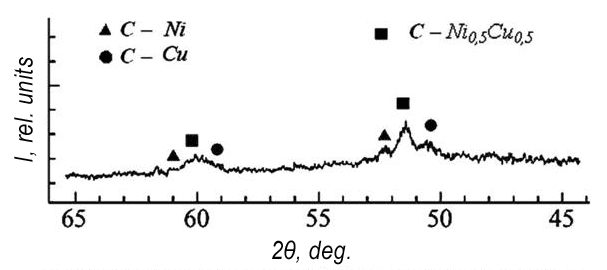
Sequential layers of magnetic / non-magnetic material in pores: XRD spectrum of Ni-Cu layers formed in pores of SiO2 layer. Reflects are registered which are attributed to the FCC-phase of nickel (unit cell parameter a = 0,352 nm), FCC-phase of copper (a = 0,362 nm) and solid solution phase of Ni0,5Cu0,5 compound with the unit cell parameter а = 0,357 nm (fig. 1).
Fig.1. Radiographs of the nickel-copper layers formed in the pores of the layer SiO2.
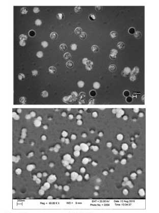
The surface has been studied of a scanning electron microscope p-Si/SiO2(Ni-Cu) heterostructure (fig. 2).
Fig.2. SEM image of the surface of p-Si/SiO2(Ni-Cu) heterostructure. This concept is possible to obtain controlled electronic material with pores in oxide on semiconductors (TEMPOS). Behavior TEMPOS-structures depends on:
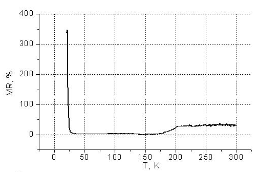
Prospects of further work with Si/SiO2/(Cu/Ni) with the goal of an amplification of the magnetoresistive effect and broadening of temperature range of its existence are concerned with a creation of sequential layers of metals in pores. For the two-layer metallic structure one can observe the MR effect (up to 40%) around room temperature (fig.3).
Fig.3. Temperature dependence of magnetoresistance for the Si/SiO2/(Cu/Ni) structure. The concept allows you to create carbon nanotubes (CNTs) on nickel clusters in the pores of the layer SiO2. On the basis of the structures of CNTs Si/SiO2/Ni possible construction of various electrical and electronic devices.
|