|
German-Belarusian Scientific Collaboration for 'Semiconductor Nanostructures for Novel Sensor and Microelectronic Devices'. Transnational cooperation between the Institute of Photonic Technology (IPHT) and the Scientific-Practical Materials Research Centre of the National Academy of Sciences of Belarus (NASB). Field of work 'Surface structuring, nanostructures growth/formation and optoelectronic device engineering'.
The beginning of cooperation - January 1, 2013, deadline - December 31, 2013.
Short Description and scientific objective:
In spite of almost 15 years of intense research on the formation and studies of semiconductor nanowires (NWs), several of the expected, significant, breakthroughs have been reached due to the influence of the nanowires structure. Semiconductor nanowires have been attracting large interest as a very promising approach toward post CMOS nano-electronics, for photonic, for energy and life science, as well as for fundamental materials science and physics studies. This is because NWs offer bottom-up or top-down self-assembly of ordered one – dimensional nanostructures (1D), creation of new combinations of hetero-junctions with sharp interfaces, including materials with large lattice mismatch, and the ability to grow semiconductor nanowires on silicon and further integration in silicon technology. Semiconductor nanowires, especially, silicon nanowires (SiNWs) are expected to possess significantly different optical properties from their bulk-length counterparts because they are smaller than the wavelength of visible light. The physical-chemical synthesis of 1D nanostructures has provided a new route to manufacture complex vertical semiconducting nanostructures with precision on the atomic scale. A major problem inhibiting the utilization of these structures and limiting the investigation of epitaxial/vertical aligned growth is finding a way to incorporate them into circuits. Elucidating German—Belarusian initiative is a complex task, which requires an interdisciplinary consortium capable of addressing all relevant issues from metal nanoparticle template formation, 1D semiconductor nanostructures growth, analysis of chemical and physical properties and device formation. In this proposal we suggest therefore a transnational cooperation between the Institute of Photonic Technology (IPHT) and the Scientific-Practical Materials Research Centre of the National Academy of Sciences of Belarus (NASB). Initially, we will synthesize from the gas phase (using low pressure chemical vapor deposition or/and metal-organic chemical vapor deposition techniques) 1D nanostructures (silicon, germanium, tin oxide, iron oxide, etc.) at specific sites with well-defined lengths and diameters. The growth of these nanostructures is determined by metal catalysis, so called vapor-liquid-solid growth approach. The control over the 1D nanostructure growth is mediated through the usage of nanoscopic metal templates. At present an intensive search for the new technologies which make it possible to lower the dimensions of electronic devices down to the nanometer size range takes place worldwide. On this concern, an interest to the development of non-traditional technologies of formation of nanomaterial and nanostructure arrays increases. In this way, the so-called swift heavy ion (SHI) track technology will be used in the proposed research. It is connected with creation of narrow trails of radiation damage (“latent SHI tracks”) as a result of high-energy ion impact. By means of dissolution of latent track material due to chemical etching pores of various forms and dimensions are formed. The etched SHI tracks can be subsequently filled (electrochemically or from gas phase, for example atomic layer deposition) with practically any material, and the embedded matter can be arranged as either massive wires or tubules, or it can be dispersed as small nanoparticles along the ion track length. The positioning of the nanoparticles will be carried out using swift heavy ion tracking and electrochemistry (holes will be filled with catalytic metals such like gold, gallium, aluminum or silver) for ‘proof of concept studies’ and anodic aluminum oxide (AAO) masks to create wafer size nano-templates or filled AAO pores using Atomic Layer Deposition (ALD) with plasmonic metals or oxides nanotubes or nanowires. Growth mechanisms and the initial stages of the VLS growth will be investigated using in-situ synthesis of individual 1D nanostructures in the scanning electron microscope (SEM). Using transmission electron microscopy (TEM) techniques, we will characterize the 1D nanostructures chemically and structurally. SEM in combination with focused ion beam (FIB), electron beam induced current (EBIC) will be used to explore structural and electrical properties of the nanostructures. Raman spectroscopy with combination of FIB technology will be used to evaluate stresses and defects in substrate after heavy ions treatment. This joint project will allow to explore semiconductor process technology combined with SHI track technology - based nanopatterning techniques to place 1D nanostructures, in new type of devices. We will explore and advance the ‘bottom-up’ approach in studying the synthesis of highly uniform (in diameter and length) 1D semiconductor nanostructures, in a vertically, perfectly aligned arrangement at predetermined sites. The consortium will provide for the required competences: IPHT growth of 1D semiconductor nanostructures, structural and physical characterization; NASB: nano-template synthesis via SHI track technology, 1D nanodevice processing and characterization. The project blocks are detailed in the following Table 1. The bilateral partner visits will take place as well as will be planned. The visit between German and Belarusian partners will permit the exchange of knowledge of partners experimental as well as characterization and simulation capabilities. Partner visits should usually last for up to a month and should include visit and work of the labs as well as giving a scientific talk at the partner site.
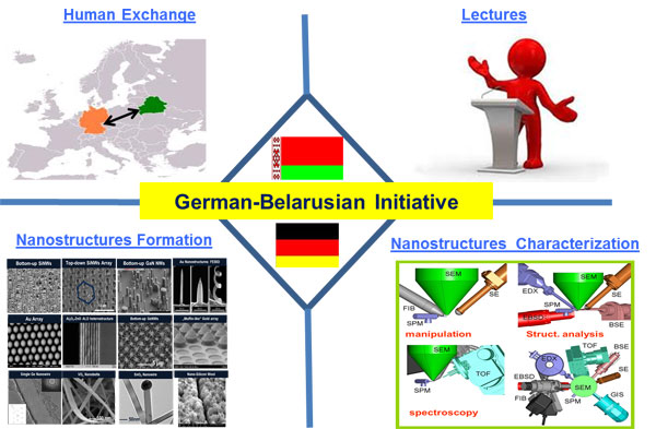
Figure 1. Schematic representation of activities during German-Belarusian initiative.
Aside of the scientific output, a major aspect of the proposal is to provide young researchers and especially PhD candidates the opportunity to ‘accompany their material’ to the different institutions to carry out specific analysis or processing tasks there. Thus, young scientists get to know not only different laboratories, but also the research culture in different European countries. The two proposals of this joint research are closely interconnected and will strongly benefit from the consortium character.
Information about organizer of the scientific collaboration: http://www.ipht-jena.de/
|


")