|
The study gas-sensitive properties of carbon nanotubes formed on the basis of the structures Si/SiO2/Ni, showed that under the action of ammonia and nitric oxide nanotubes are changing the value of the conductivity in different directions - the interaction of NH3 with the conductivity decreases and the interaction with NO2 increases. This is due to charge interaction with the outer walls of nanotubes adsorbed molecules, which may be due to the doping of carbon nanotubes with electrons in the process of physical adsorption of molecules NH3. |
|
Read more...
|
|
|
The study field emission properties of carbon nanotubes formed on the basis of the structures Si/SiO2/Ni, showed the promise of their use as cathodes in field emission and low threshold for long-term stability.
Revealed high stability of emission current and the luminosity of the screen and the cathode on the basis of the structure Si/SiO2/Ni with CNTs. Current change during the measurement (5 hours) did not exceed 8%, its highest stability was observed at an interelectrode distance of 1 mm. |
|
Read more...
|
|
Carbon nanotubes and SiC whiskers in the pyrolysis of vapors of acetonitrile on nickel clusters deposited in the pores obtained with dressings tracks of heavy metal ions in the dielectric layers of SiO2 with single-crystal silicon substrates. The resulting structures were investigated by scanning electron microscopy and Raman spectroscopy, field emission characteristics are measured them. |
|
Read more...
|
|
TEMPOS (Tunable Electronic Material in Pores in Oxide on Semiconductors) structures exhibit properties similar to the properties of electronic devices such as MOS structures with nonlinear volt-ampere characteristics, including negative differential resistance. At the same time TEMPOS-structures have the additional free parameters such as shape and density of etched tracks, position, height, diameter, and type of material that is embedded in the tracks. |
|
Read more...
|
|
Tasks of the modern technology are concerned not only with the use and improvement of conventional methods of micron- and submicron-scale structures fabrication, but with a development of new principles and technological processes of the creation of nanoelectronic devices. In this concern an interest to structures created by swift heavy ion (SHI) track technology obvious.
The Si/SiO2/Metal nanostructure was formed with the use of the SHI track technology. By means of this technology a matrix with statistically uniform distribution of latent SHI tracks in a silicon dioxide layer has been created. After chemical etching ion tracks were transformed in pores having form of frustums with an average diameter 150 nm and height corresponding to SiO2 layer thickness (200 nm). In this nanoporous matrix alternating layers (each layer thickness ~10 nm) of ferromagnetic (Ni) and nonmagnetic (Cu) metals was electrochemically deposited. |
|
Read more...
|
|
Based on flexible polymer films with the tracks of swift heavy ions can be created by different nano-and microelectronic devices:
- temperature, pressure, humidity, magnetic field and light radiation sensors
- microelectrotecnical devices (microtransformer, microcapacitor etc.)
- integrated microcircuits on a flexible basis
- advanced storage information systems
|
|
Read more...
|
|
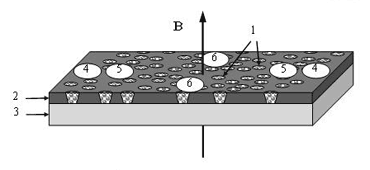
Using the swift heavy ion tracks, a structure n-Si/SiO2/Ni (fig.1). A schematic diagram of contacts placement on the Si/SiO2/Metal structure for measurements of electrical-physical and galvanomagnetic properties:
|
|
|
Fig.1. Schematic representation of Si/SiO2/Metal structure: 1 – Metal in pores; 2 – Silicon oxide layer; 3 – Silicon substrate; 4 – Current contacts; 5 – Potential contacts; 6 – Hall contacts
|
|
|
Read more...
|
|
|
<< Start < Prev 1 2 3 4 Next > End >>
|
|
Page 4 of 4 |


")