
")
| Investigations of the structural characteristic features of Si/SiO2/Metal (Ni, Cu) systems |
|
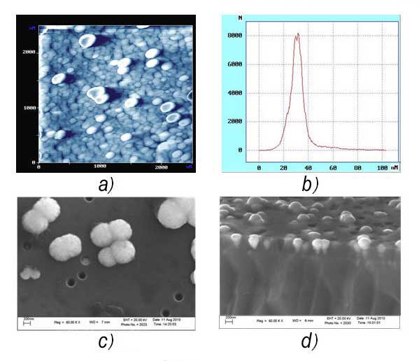
Atomic force microscopy (AFM) images of the surface of n-Si/SiO2/Ni sample irradiated by 197Au26+ ions with energy 350 MeV and fluence 5×108 cm-2: (а) – phase-contrast image; (b) – distribution bar chart of nickel ougrowth heights within the scanned region.
SEM images of n-Si/SiO2/Ni sample, irradiated by 131Xe17+ ions with energy 350 MeV and fluence 5×108 cm-2: (c) top view; (d) cross-sectional view.
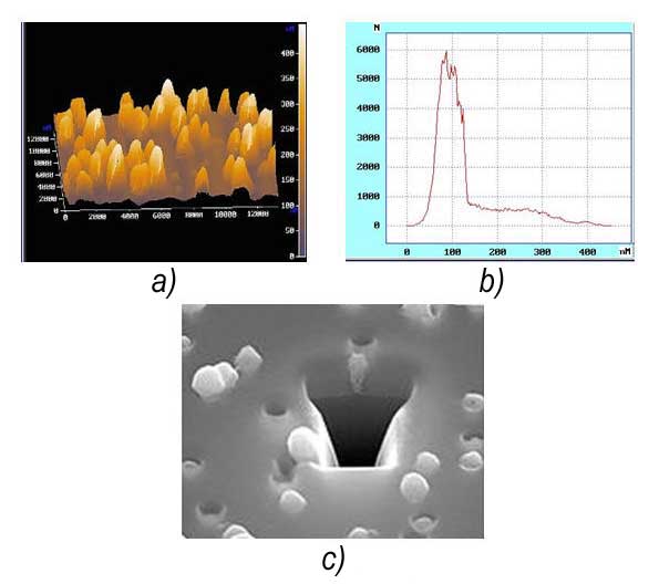
AFM images of n-Si/SiO2/Cu sample, irradiated by 197Au26+ ions with energy 350 MeV and fluence 5×108 cm-2: (а) phase-contrast image; (b) distribution bar chart of copper ougrowth heights within the scanned region.
(c) SEM image of the n-Si/SiO2/Cu sample irradiated by 131Xe17+ ions with energy 350 MeV and fluence 5×108 cm-2 after its shearing by the focused ion beam. The image was obtained by the “Cross-section” method.
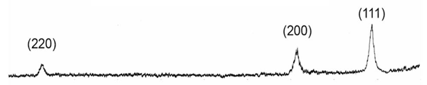
Reflexes (220), (200) and (111) which are characteristic for polycrystalline metallic nickel. Ni crystallites are deposited in the form of nanoclusters with dimensions 30-50 nm which are stochasticlly oriented in the pore. A formation of FCC Ni phase with a characteristic unit cell parameter a = 0.352 nm takes place during the electrodeposition.
|